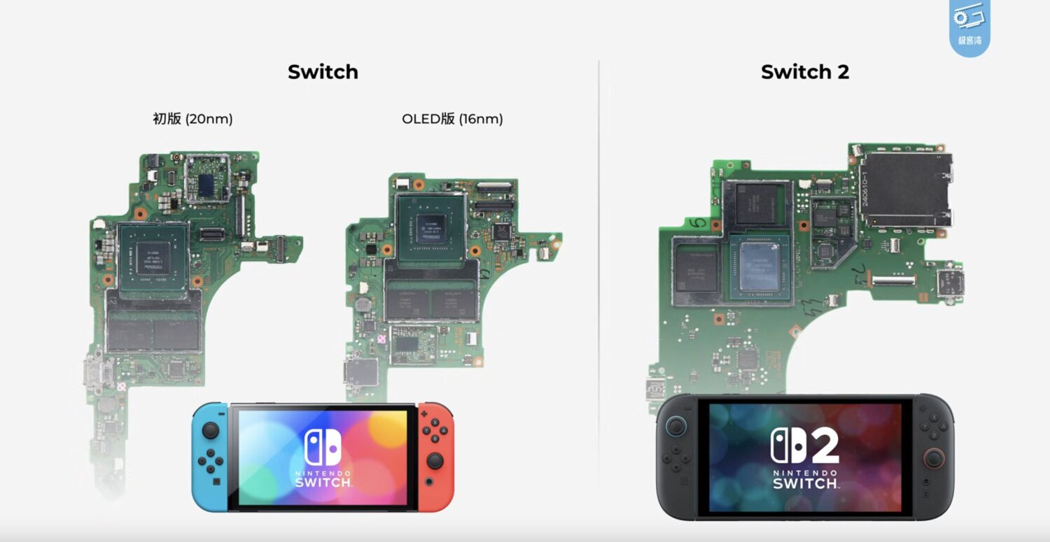
In a landmark moment for hardware enthusiasts, the Nintendo Switch 2 motherboard has been obtained and meticulously analyzed by Chinese YouTuber Geekerwan, providing an early and verifiable look at the next-generation Nintendo hardware just weeks before its official launch.
This analysis has illuminated core specifications and manufacturing details, offering enthusiasts and industry watchers a rare glimpse into the engineering advances behind the Nintendo Switch 2.
Geekerwan acquired the Nintendo Switch 2 motherboard in China for approximately 1000 RMB (about USD 139).
Notably, the design closely matches an earlier leak from 2024, lending further authenticity to the findings.
The Switch 2 motherboard is markedly larger than its predecessor, signifying architecture changes intended to accommodate upgraded hardware.
Notably, the game card slot is now directly integrated onto the motherboard, differing from the modular design found in the original Nintendo Switch.
The technical analysis highlighted several important component upgrades.
Storage duties are now handled by a Hynix 256GB UFS 3.1 chip, promising faster and more efficient data access compared to the previous Nintendo Switch models.
Wireless connectivity comes courtesy of a MediaTek Wi-Fi/Bluetooth module, while a Little Crab audio chip rounds out significant onboard enhancements.
Power delivery for the new system-on-chip (SoC) is rated at 34.4W, marking an increase over the prior generation and potentially supporting higher performance and greater resource demands.
Laboratory examinations have verified that the motherboard was produced in early September 2024 (the 36th week of the year), confirming its currency and relevance to the upcoming console release.
The crown jewel of this motherboard is its SoC: after years of rumors, it is now confirmed that the Switch 2 uses a bespoke Tegra T239 SoC.
In terms of die surface area, the Switch 2 SoC measures 207 mm², significantly larger than the 100 mm² and 118 mm² footprints of the original and second-generation Switch models, respectively.
For context, it's even slightly larger than the GA107 chip found in the RTX 3050 Ti, highlighting Nintendo’s commitment to closing the technological gap with contemporary portable and console hardware.
The manufacturing process for the Switch 2 SoC is a global effort led by Samsung, with packaging handled in Taiwan.
Production records indicate the SoC was manufactured in late May 2024, and it's understood that the chip design was finalized, or 'taped out,' in 2021—evidence that supports prior reports suggesting a delayed hardware rollout owing to software development timelines.
Detailed technical scrutiny further reveals the SoC is produced using a combination of Samsung’s 8nm and 10nm processes, with five major chip components using 10nm nodes and two using 8nm nodes.
According to Geekerwan’s review, this hybrid approach is not expected to impact performance, as both node technologies share similar performance characteristics.
With these confirmed details, anticipation for the Nintendo Switch 2 continues to mount as its launch date approaches.
Nintendo’s strategic hardware innovations, underscored by partnerships with industry leaders such as Samsung, MediaTek, and Hynix, set the stage for a new era in hybrid gaming.
As always, Nintendo’s ability to blend efficiency, innovation, and global manufacturing expertise is poised to redefine expectations for the gaming community on the Nintendo Switch 2.